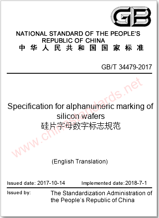
GB/T 34479-2017 in English
VALIDSpecification for alphanumeric marking of silicon wafers
- Issued on:2017-10-14
- Implemented on:2018-07-01
- File Format:PDF
- Delivery:Via email within 1~3 business days
$204.00
| Standard No: | GB/T 34479-2017 |
| Document status: | VALID |
| Title in English: | Specification for alphanumeric marking of silicon wafers |
| Title in Chinese: | 硅片字母数字标志规范 |
| Language: | English |
| File Format: | Electronic (PDF) |
| Delivery: | Via email within 1~3 business days |
| Issued on: | 2017-10-14 |
| Implemented on: | 2018-07-01 |
| ICS Classification: | 29.045-Semiconducting materials |
| Chinese Classification: | H80-Semimetal and semiconductor material in general |
| Professional Classification: | GB-National Standard |
| Related Keywords: | silicon wafer alphanumeric marking specification
silicon wafers silicon wafers introduction silicon wafer identification alphanumeric marking |
| Related Topics: | digital light film
silicon wafer letter Alphabet wave number letter digital sign content letter word count Silicon number peak number letter letters of the second Number of slices letter next to the word GBT34479 GB/T 34479-2017 |
《GB/T 34479-2017硅片字母数字标志规范》由TC203(全国半导体设备和材料标准化技术委员会)归口,主管部门为国家标准化管理委员会。
Introduction
1. Background and significance of standard formulation
GB/T 34479-2017 "Silicon Wafer Alphanumeric Marking Specification" is to unify and standardize the silicon wafer identification in the semiconductor industry to ensure consistency and traceability during production, testing and use. The standard was proposed by the National Technical Committee for Semiconductor Equipment and Materials Standardization and promoted and applied nationwide.
2. Standard framework and core content
| Dimensions | Specific requirements | Scope of application |
|---|---|---|
| Marking Coding Specification | Specifies the encoding rules of 18 characters, including supplier identification code, dopant type and other information. | Applicable to silicon wafers with diameters of 100mm, 125mm, 150mm and 200mm. |
| Character size and spacing | Specify the specific values of character height, width, thickness and spacing to ensure the reliability of automatic optical character reading (OCR). | Different requirements are proposed for silicon wafers with reference surfaces and cutouts. |
| Error code detection method | Ensure data integrity and accuracy through recursive algorithms and check character generation rules. | Applicable to the verification process of all labeled information. |
3. Technological evolution and practical application
Technical background:With the rapid development of the semiconductor industry, the specifications and quality requirements of silicon wafers are constantly improving. Unified identification specifications have become an important part of industry standardization.
Actual case:A semiconductor manufacturing company has significantly improved OCR reading efficiency and reduced product return rates due to identification errors by adopting the GB/T 34479 standard.
4. Implementation suggestions
- Training and promotion:Organize relevant personnel to learn the content of the standard to ensure that they are understood and implemented in place.
- Equipment calibration:Regularly calibrate the OCR equipment to ensure that it meets the character recognition requirements in the standard.
- Data management: Establish a complete database management system to record the identification information of all silicon wafers for easy traceability and analysis.

Loading PDF document...
Error loading PDF. Please make sure the file is valid and try again.
We also recommend
-

GB/T 43612-2023 in English
Collection of metallographs on defects in silicon carbide crystal materials
2023-12-28 -

GB/T 6617-2009 in English
Test method for measuring resistivity of silicon wafer using spreading resistance probe
2009-10-30 -

GB/T 29505-2013 in English
Test method for measuring surface roughness on planar surfaces of silicon wafer
2013-05-09 -

GB/T 24574-2009 in English
Test methods for photoluminescence analysis of single crystal silicon for Ⅲ-Ⅴ impurities
2009-10-30 -

GB/T 4058-2009 in English
Test method for detection of oxidation induced defects in polished silicon wafers
2009-10-30 -

GB/T 1554-2009 in English
Testing method for crystallographic perfection of silicon by preferential etch techniques
2009-10-30 -

GB/T 37051-2018 in English
Test method for determination of crystal defect density in PV silicon ingot and wafer
2018-12-28 -

GB/T 16595-2019 in English
Specification for a universal wafer grid
2019-03-25 -

GB/T 26066-2010 in English
Practice for shallow etch pit detection on silicon
2011-01-01


